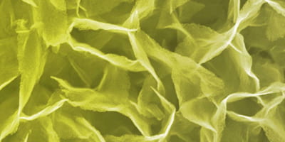
- Scanning Electron Microscopy
- Transmission Electron Microscopy
- Cryo-Electron Microscopy
- X-RAY Microanalysis
- X-Ray Photoelectron Spectroscopy
- X-Ray Diffraction
- Small & Wide Angle X-Ray Scattering
- X-RAY Fluorescence
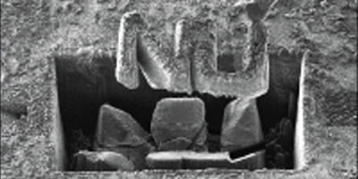
- Focused Ion Beam
- Atom Probe Tomography
- Secondary Ion Mass Spectrometry
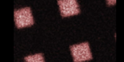
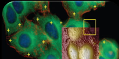
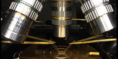
- Optical Microscopy
- Raman Spectroscopy
- Ultraviolet Photoelectron Spectroscopy
- Fourier Transform Infrared Spectroscopy (FTIR)
- Ellipsometry & Reflectometry
- Dynaic Light Scattering (DLS)
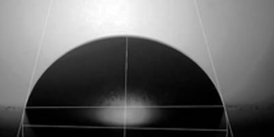
- Contact Angle Measurement
- Atomic Force Microscopy
- Nanoindentation
- Correlative Fluidic AFM/Optical Microscopy
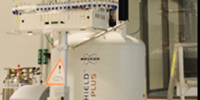
- Nuclear Magnetic Resonance (NMR)
- Mass Spectrometry
- Indutively Coupled Plasma Atomic Emission Spectroscopy
- High Performance Liquid Chromatography
- Electrical Probe Station
- In Situ SEM Nanoprobe
- Hall Effect Measurement
- Sample Coating
- Ion Beam Thinning
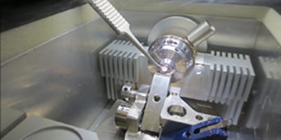
- Mechanical Polishing
- Plasma Cleaning
- Electropolishing
- Cryogenic Sample Preparation
- Lyophilization
- Photolithography
- Electron Beam Lithography
- Ion Beam Lithography
- Parallel Pen Lithography
- Physical Vapor Deposition
- Chemical Vapor Deposition
- Parylene Coating
- Atomic Layer Deposition
- Reactive Ion Etching
- Vapor Etching
- Plasma Ashing
- Wet Etching
- Critical Point Drying
- Thermal Processing
- Wafer Dicing
- Vacuum Packaging
- Wire Bonding
- Wafer Binding